GHENT — As the cornerstone of modern technology, semiconductor manufacturing plays a pivotal role in the devices that power everyday life. However, with ever-smaller chips and increasingly complex designs, the challenge of detecting even the tiniest defects has become a monumental task. Traditional inspection methods, reliant on manual checks and rule-based systems, are struggling to keep pace with this evolution. Enter Robovision 5.7—an AI-powered vision platform poised to transform semiconductor manufacturing by delivering unparalleled defect detection accuracy and adaptability.
Semiconductor fabrication relies on lithography, where intricate circuits are etched onto silicon wafers. The process demands pinpoint precision, as even the smallest flaw can result in a defective chip. Historically, semiconductor fabs have depended on manual inspection and rule-based defect detection systems, which, while effective, are reaching their limits as chip designs grow more intricate and defects evolve.
Robovision 5.7 leverages deep learning to address this challenge, moving beyond static rules to a dynamic, self-improving system. The platform continuously learns from the defects it encounters, improving its ability to detect and classify them with far greater precision than human operators or traditional systems could ever achieve.
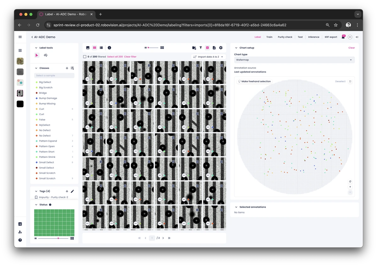
One of the standout features of Robovision 5.7 is its introduction of the Split View interface. This new feature allows engineers to view wafer maps and defect images side-by-side, simplifying the defect identification and classification process. No longer will operators need to toggle between screens or sift through vast amounts of data—everything is presented clearly, allowing them to focus on improving yield.
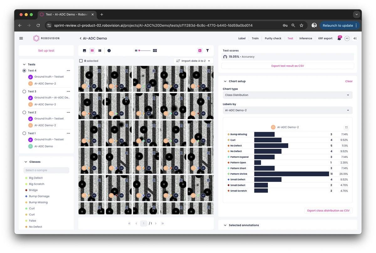
But Robovision 5.7 goes beyond just identifying defects—it introduces the Purity Loop, a continuous improvement cycle that ensures the AI model consistently improves its accuracy. This loop helps the system identify inconsistencies between human-labeled data and AI-generated classifications, enabling it to self-correct and refine its model. The result is a platform that becomes more accurate over time, providing semiconductor manufacturers with a trustworthy, high-precision defect classification system.
Traditional defect detection systems often struggle to adapt to the evolving nature of semiconductor defects. As new materials and complex 3D geometries are introduced in chip designs, the types of defects encountered are constantly changing. Robovision 5.7’s deep learning algorithms are specifically designed to adapt to these shifts, making it the ideal solution for fabs working with cutting-edge technologies.
Not only does Robovision 5.7 improve the accuracy of defect detection, but it also speeds up the inspection process. By automating defect classification, the platform reduces inspection times and minimizes human error, which leads to higher yields and reduced costs. With the ability to analyze images in real-time, Robovision 5.7 helps semiconductor fabs optimize workflows and improve overall operational efficiency.
Scalability is another key strength of Robovision 5.7. As semiconductor manufacturers expand operations and increase the number of production lines, they need solutions that can easily scale. Robovision 5.7 offers a customizable platform that seamlessly integrates into existing workflows across multiple fabs and production lines, ensuring minimal disruption and maximum flexibility.
As the semiconductor industry continues to evolve, Robovision 5.7 stands at the forefront of innovation, delivering a future-proof solution for defect detection. With its deep learning-powered platform, continuous improvement cycles, and adaptability to new technologies, Robovision 5.7 empowers semiconductor manufacturers to stay ahead of the curve, enhance yield, reduce costs, and optimize production processes.
In this age of microscopic precision, where even the smallest flaw can have monumental consequences, Robovision 5.7 is not just a tool—it’s a game changer, transforming the semiconductor manufacturing process and enabling manufacturers to meet the demands of tomorrow’s technologies.