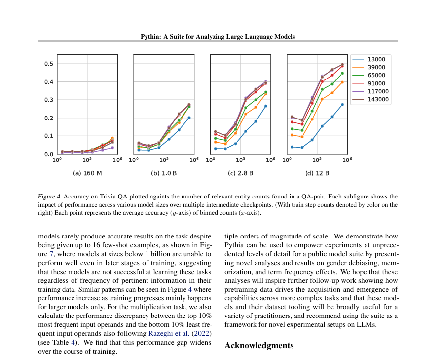

HOBOKEN, NJ — Quantum Computing Inc. (QCi), a leader in integrated photonics and quantum optics, has announced the receipt of its fifth purchase order for its thin film lithium niobate (TFLN) photonic chip foundry. The latest order comes from a Canadian research team focused on advancing quantum photonics, marking another significant milestone in QCi’s ongoing efforts to drive innovation in this field.
Under the terms of the order, QCi will provide the research group with custom test structures based on its TFLN photonic integrated circuit (PIC) chip technology. These structures will serve as a foundation for developing more advanced components, such as periodically poled lithium niobate (PPLN) elements, which play a crucial role in generating entangled photons and enabling optical frequency conversion. Additionally, the agreement grants the research team priority access to future multi-project wafer (MPW) runs from QCi, ensuring efficient development and manufacturing.
Dr. William McGann, CEO of QCi, expressed his enthusiasm about the collaboration, stating, “We are thrilled to support this research team’s groundbreaking work by offering our TFLN foundry services. This partnership highlights the growing demand for the energy efficiency and scalability of TFLN technology, demonstrating its potential to tackle real-world challenges and reshape next-generation photonics and quantum technology.”
In line with this development, QCi has also recently launched its Photonic Integrated Circuit (PIC) Process Design Kit (PDK), utilizing GDSFactory’s open-source platform. This Python-based tool is widely used across the commercial and research sectors and allows users to design complex systems, including photonic circuits. By hosting QCi’s PDK on GDSFactory’s platform, users can design and simulate their intended circuits before submitting their final designs for manufacturing. This initiative is expected to streamline the design and production process, particularly in preparation for QCi’s upcoming MPW runs.
The availability of the PDK will increase accessibility for customers in the photonics market, and QCi plans to expand the service through additional providers over the next two years. This week, QCi is set to showcase its PDK at SPIE Photonics West 2025, the world’s largest event for photonics technologies, to further promote its innovative solutions.
With multiple pre-orders secured through its Pilot Launch Program, including partnerships with a leading European technical university and a Canadian PIC design house, QCi is expanding its reach. Furthermore, its new U.S.-based chip foundry in Tempe, Arizona, is set to begin operations this quarter, enhancing the company’s capacity to produce TFLN-based PICs and nanophotonic devices, cementing its position in the growing optical chip market.
For more information about QCi’s foundry and its collaborative opportunities, visit the QCi Foundry webpage.